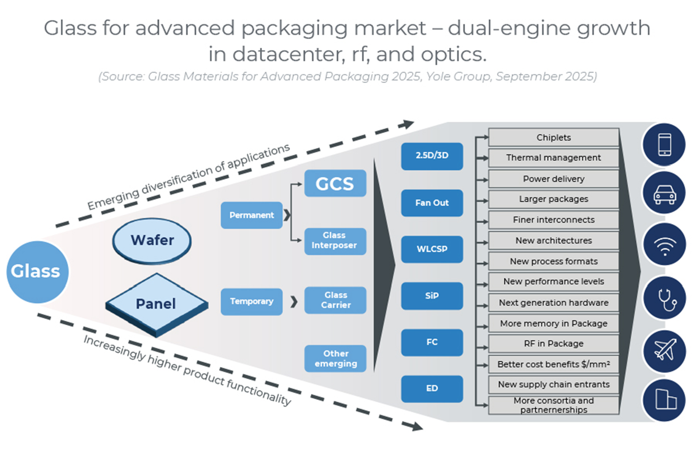
Glass is rapidly becoming a platform material for terminal markets led by data centers and telecommunications. Within data centers, it underpins two key packaging carriers: chip architectures and optical input/output (I/O).
Its low coefficient of thermal expansion (CTE) and deep ultraviolet (DUV)-compatible glass carriers have enabled hybrid bonding and 300 mm thin-wafer backside processing to become standardized manufacturing flows.
As switch and accelerator modules grow beyond wafer-stepper dimensions, panel carriers are becoming indispensable. The market for glass core substrates (GCS) is projected to reach $460 million by 2030, with optimistic forecasts suggesting mainstream adoption around 2027–2028. Meanwhile, glass interposers are expected to exceed $400 million even under conservative projections, and the steady glass carrier segment represents a market of around $500 million.
In advanced packaging, glass has evolved from being a simple component to becoming a platform business. For glass carriers, revenue generation is shifting from per-panel pricing to per-cycle economics, where profitability depends on reuse cycles, laser/UV debonding yields, process yield, and edge damage mitigation. This dynamic benefits suppliers offering CTE-graded portfolios, bundle providers selling integrated stacks of carrier + adhesive/LTHC + debond, and regional reclaim vendors specializing in optical-quality assurance.
Companies with deep glass expertise—such as Plan Optik, known for its high-flatness carriers with engineered edge geometries and controlled transmission—are optimally positioned in this value chain.
Glass core substrates are now unlocking display panel manufacturing capacity into profitability through TGV (Through Glass Via), fine RDL (Redistribution Layer), and build-up processes. Market leaders are those mastering the critical interfaces:
-
High-yield TGV drilling/etching
-
Void-free copper filling
-
Panel lithography with adaptive alignment
-
2/2 µm L/S (line/space) patterning
-
Warp-controllable panel handling technologies
Substrate and OSAT vendors collaborating with display glass manufacturers are converting large-area capacity into cost advantages for panel-scale packaging.
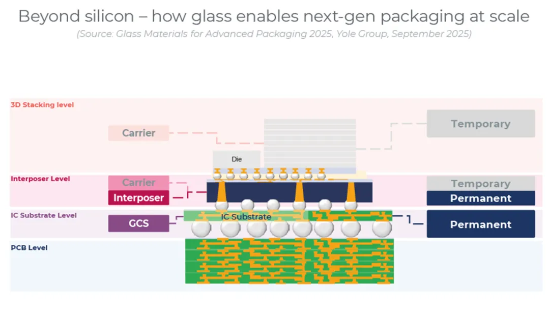
From Carrier to Full-Fledged Platform Material
Glass has transformed from a temporary carrier into a comprehensive material platform for advanced packaging, aligning with megatrends such as chiplet integration, panelization, vertical stacking, and hybrid bonding—while simultaneously tightening budgets for mechanical, thermal, and cleanroom performance.
As a carrier (both wafer and panel), transparent, low-CTE glass enables stress-minimized alignment and laser/UV debonding, improving yields for sub-50 µm wafers, backside process flows, and reconstituted panels, thus achieving multi-use cost efficiency.
As a glass core substrate, it replaces organic cores and supports panel-level manufacturing.
-
TGVs provide dense vertical power and signal routing.
-
SAP RDL pushes wiring limits to 2/2 µm.
-
Flat, CTE-tunable surfaces minimize warpage.
-
Optical transparency prepares the substrate for co-packaged optics (CPO).
Meanwhile, heat dissipation challenges are addressed through copper planes, stitched vias, backside power delivery networks (BSPDN), and double-sided cooling.
As a glass interposer, the material succeeds under two distinct paradigms:
-
Passive mode, enabling massive 2.5D AI/HPC and switch architectures that achieve wiring density and bump counts unattainable by silicon at comparable cost and area.
-
Active mode, integrating SIW/filters/antennas and metalized trenches or laser-written waveguides within the substrate, folding RF paths and routing optical I/O to the periphery with minimal loss.
Market Outlook and Industry Dynamics
According to the latest analysis by Yole Group, glass materials have become central to the semiconductor packaging revolution, driven by major trends in artificial intelligence (AI), high-performance computing (HPC), 5G/6G connectivity, and co-packaged optics (CPO).
Analysts emphasize that glass’s unique properties—including its low CTE, superior dimensional stability, and optical transparency—make it indispensable for meeting the mechanical, electrical, and thermal requirements of next-generation packages.
Yole further notes that data centers and telecom remain the primary growth engines for glass adoption in packaging, while automotive, defense, and high-end consumer electronics contribute additional momentum. These sectors increasingly depend on chiplet integration, hybrid bonding, and panel-level manufacturing, where glass not only enhances performance but also reduces total cost.
Finally, the emergence of new supply chains in Asia—particularly in China, South Korea, and Japan—is identified as a key enabler for scaling production and strengthening the global ecosystem for advanced packaging glass.
Post time: Oct-23-2025