Why modern chips run hot
As nanoscale transistors switch at gigahertz rates, electrons rush through circuits and lose energy as heat—the same heat you feel when a laptop or phone gets uncomfortably warm. Packing more transistors onto a chip leaves less room to remove that heat. Instead of spreading evenly through silicon, heat accumulates into hotspots that can be tens of degrees hotter than surrounding regions. To avoid damage and performance loss, systems throttle CPUs and GPUs when temperatures spike.
The scope of the thermal challenge
What began as a race to miniaturize has become a battle with heat across all electronics. In computing, performance keeps pushing power density higher (individual servers can draw on the order of tens of kilowatts). In communications, both digital and analog circuits demand higher transistor power for stronger signals and faster data. In power electronics, better efficiency is increasingly limited by thermal constraints.
A different strategy: spread heat inside the chip
Rather than letting heat concentrate, a promising idea is to dilute it within the chip itself—like pouring a cup of boiling water into a swimming pool. If heat is spread right where it’s generated, the hottest devices stay cooler and conventional coolers (heat sinks, fans, liquid loops) work more effectively. This requires a high-thermal-conductivity, electrically insulating material integrated just nanometers from active transistors without disturbing their delicate properties. An unexpected candidate fits this bill: diamond.
Why diamond?
Diamond is among the best thermal conductors known—several times higher than copper—while also being an electrical insulator. The catch is integration: conventional growth methods require temperatures around or above 900–1000 °C, which would damage advanced circuitry. Recent advances show that thin polycrystalline diamond films (only a few micrometers thick) can be grown at much lower temperatures suitable for finished devices.
Today’s coolers and their limits
Mainstream cooling focuses on better heat sinks, fans, and interface materials. Researchers also explore microfluidic liquid cooling, phase-change materials, and even immersing servers in thermally conductive, electrically insulating liquids. These are important steps, but they can be bulky, expensive, or poorly matched to emerging 3D-stacked chip architectures, where multiple silicon layers behave like a “skyscraper.” In such stacks, every layer must shed heat; otherwise hotspots are trapped inside.
How to grow device-friendly diamond
Single-crystal diamond has extraordinary thermal conductivity (≈2200–2400 W m⁻¹ K⁻¹, about six times that of copper). Easier-to-make polycrystalline films can approach these values when sufficiently thick—and are still superior to copper even when thinner. Traditional chemical vapor deposition reacts methane and hydrogen at high temperature, forming vertical diamond nanocolumns that later merge into a film; by then the layer is thick, stressed, and prone to cracking.
Lower-temperature growth demands a different recipe. Simply turning down the heat yields conductive soot rather than insulating diamond. Introducing oxygen continuously etches non-diamond carbon, enabling large-grain polycrystalline diamond at ~400 °C, a temperature compatible with advanced integrated circuits. Just as importantly, the process can coat not only horizontal surfaces but also sidewalls, which matters for inherently 3D devices.
Thermal boundary resistance (TBR): the phonon bottleneck
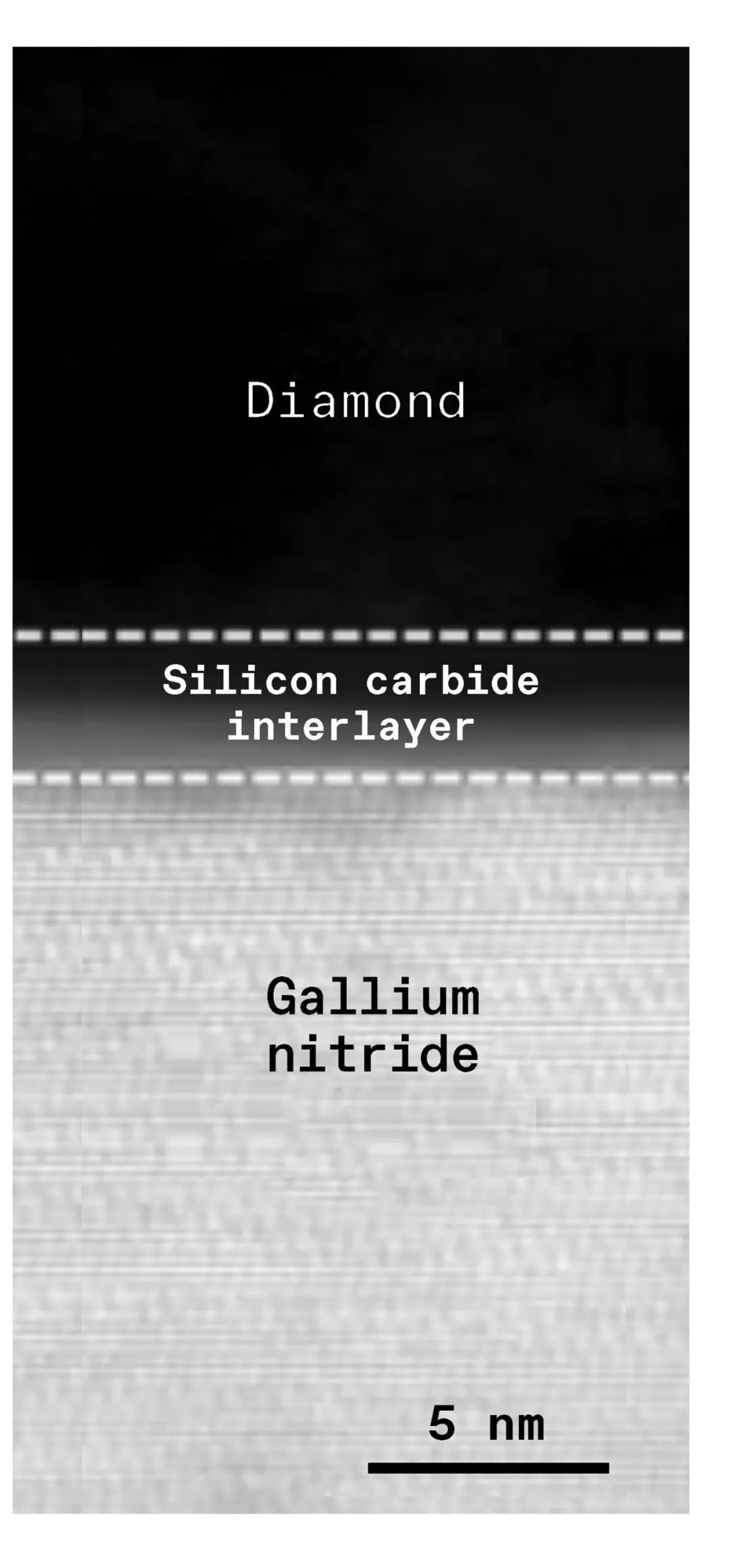
Heat in solids is carried by phonons (quantized lattice vibrations). At material interfaces, phonons can reflect and pile up, creating thermal boundary resistance (TBR) that impedes heat flow. Interface engineering seeks to lower TBR, but choices are limited by semiconductor compatibility. At certain interfaces, intermixing can form a thin silicon carbide (SiC) layer that better matches phonon spectra on both sides, acting as a “bridge” and reducing TBR—thus improving heat transfer from devices into diamond.
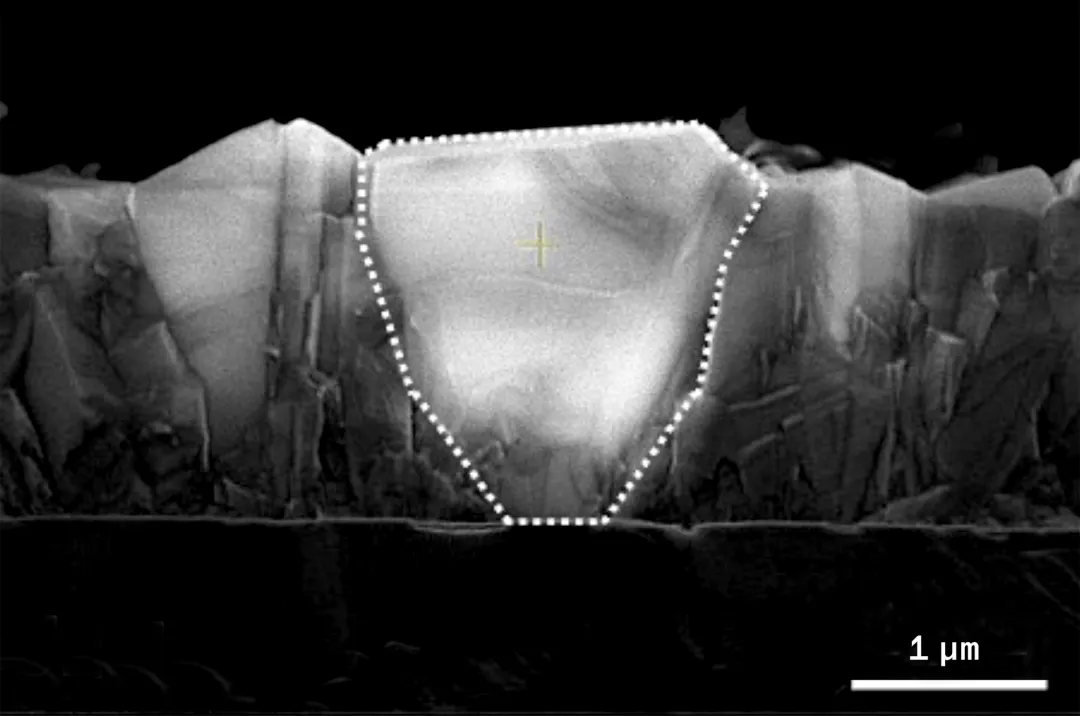
A testbed: GaN HEMTs (radio-frequency transistors)
High-electron-mobility transistors (HEMTs) based on gallium nitride control current in a 2D electron gas and are prized for high-frequency, high-power operation (including X-band ≈8–12 GHz and W-band ≈75–110 GHz). Because heat is generated very near the surface, they are an excellent probe of any in-situ heat-spreading layer. When thin diamond encapsulates the device—including sidewalls—channel temperatures have been observed to drop by ~70 °C, with substantial improvements in thermal headroom at high power.
Diamond in CMOS and 3D stacks
In advanced computing, 3D stacking increases integration density and performance but creates internal thermal bottlenecks where traditional, external coolers are least effective. Integrating diamond with silicon can again produce a beneficial SiC interlayer, yielding a high-quality thermal interface.
One proposed architecture is a thermal scaffold: nanometer-thin diamond sheets embedded above transistors within the dielectric, connected by vertical thermal vias (“heat pillars”) made of copper or additional diamond. These pillars pass heat from layer to layer until it reaches an external cooler. Simulations with realistic workloads show that such structures can reduce peak temperatures by up to an order of magnitude in proof-of-concept stacks.
What remains difficult
Key challenges include making the top surface of diamond atomically flat for seamless integration with overlying interconnects and dielectrics, and refining processes so thin films maintain excellent thermal conductivity without stressing the underlying circuitry.
Outlook
If these approaches continue to mature, in-chip diamond heat spreading could substantially relax thermal limits in CMOS, RF, and power electronics—allowing higher performance, greater reliability, and denser 3D integration without the usual thermal penalties.
Post time: Oct-23-2025