In 1965, Intel co-founder Gordon Moore articulated what became “Moore’s Law.” For over half a century it underpinned steady gains in integrated-circuit (IC) performance and declining costs—the foundation of modern digital technology. In short: the number of transistors on a chip roughly doubles every two years.
For years, progress tracked that cadence. Now the picture is changing. Further shrinkage has grown difficult; feature sizes are down to just a few nanometers. Engineers are running into physical limits, more complex process steps, and rising costs. Smaller geometries also depress yields, making high-volume production harder. Building and operating a leading-edge fab demands immense capital and expertise. Many therefore argue Moore’s Law is losing steam.
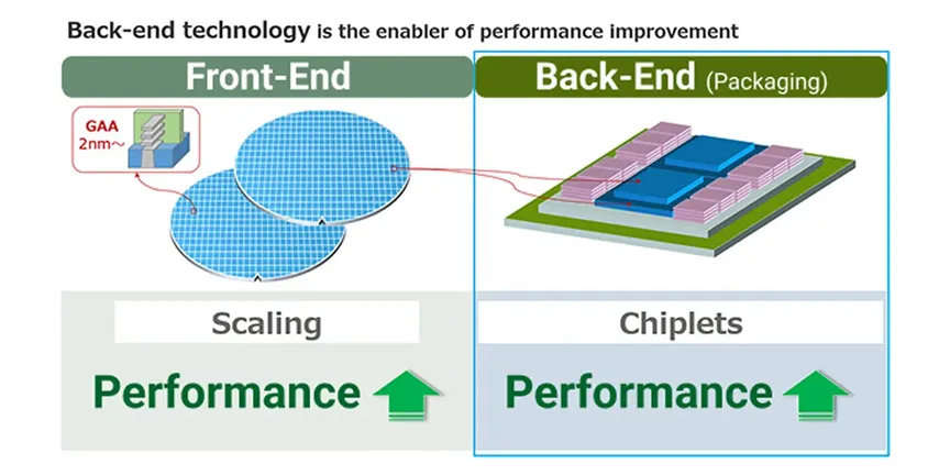
That shift has opened the door to a new approach: chiplets.
A chiplet is a small die that performs a specific function—essentially a slice of what used to be one monolithic chip. By integrating multiple chiplets in a single package, manufacturers can assemble a complete system.
In the monolithic era, all functions lived on one large die, so a defect anywhere could scrap the whole chip. With chiplets, systems are built from “known-good die” (KGD), dramatically improving yield and manufacturing efficiency.
Heterogeneous integration—combining dies built on different process nodes and for different functions—makes chiplets especially powerful. High-performance compute blocks can use the latest nodes, while memory and analog circuits stay on mature, cost-effective technologies. The result: higher performance at lower cost.
The auto industry is particularly interested. Major automakers are using these techniques to develop future in-vehicle SoCs, with mass adoption targeted after 2030. Chiplets let them scale AI and graphics more efficiently while improving yields—boosting both performance and functionality in automotive semiconductors.
Some automotive parts must satisfy stringent functional-safety standards and thus rely on older, proven nodes. Meanwhile, modern systems such as advanced driver-assistance (ADAS) and software-defined vehicles (SDVs) demand far more compute. Chiplets bridge that gap: by combining safety-class microcontrollers, large memory, and powerful AI accelerators, manufacturers can tailor SoCs to each automaker’s needs—faster.
These advantages extend beyond autos. Chiplet architectures are spreading into AI, telecom, and other domains, accelerating innovation across industries and fast becoming a pillar of the semiconductor roadmap.
Chiplet integration depends on compact, high-speed die-to-die connections. The key enabler is the interposer—an intermediate layer, often silicon, beneath the dies that routes signals much like a tiny circuit board. Better interposers mean tighter coupling and faster signal exchange.
Advanced packaging also improves power delivery. Dense arrays of tiny metal connections between dies provide ample paths for current and data even in tight spaces, enabling high-bandwidth transfer while making efficient use of limited package area.
Today’s mainstream approach is 2.5D integration: placing multiple dies side-by-side on an interposer. The next leap is 3D integration, which stacks dies vertically using through-silicon vias (TSVs) for even higher density.
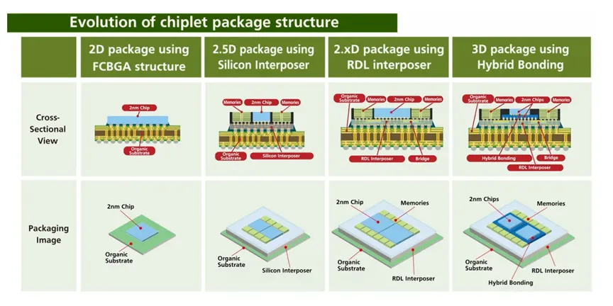
Combining modular chip design (separating functions and circuit types) with 3D stacking yields faster, smaller, more energy-efficient semiconductors. Co-locating memory and compute delivers huge bandwidth to large datasets—ideal for AI and other high-performance workloads.
Vertical stacking, however, brings challenges. Heat accumulates more readily, complicating thermal management and yield. To address this, researchers are advancing new packaging methods to better handle thermal constraints. Even so, momentum is strong: the convergence of chiplets and 3D integration is widely viewed as a disruptive paradigm—poised to carry the torch where Moore’s Law leaves off.
Post time: Oct-15-2025