A Comprehensive Overview of Monocrystalline Silicon Growth Methods
1. Background of Monocrystalline Silicon Development
The advancement of technology and the growing demand for high-efficiency smart products have further solidified the core position of the integrated circuit (IC) industry in national development. As the cornerstone of the IC industry, semiconductor monocrystalline silicon plays a vital role in driving technological innovation and economic growth.
According to data from the International Semiconductor Industry Association, the global semiconductor wafer market reached a sales figure of $12.6 billion, with shipments growing to 14.2 billion square inches. Moreover, the demand for silicon wafers continues to rise steadily.
However, the global silicon wafer industry is highly concentrated, with the top five suppliers dominating over 85% of the market share, as shown below:
-
Shin-Etsu Chemical (Japan)
-
SUMCO (Japan)
-
Global Wafers
-
Siltronic (Germany)
-
SK Siltron (South Korea)
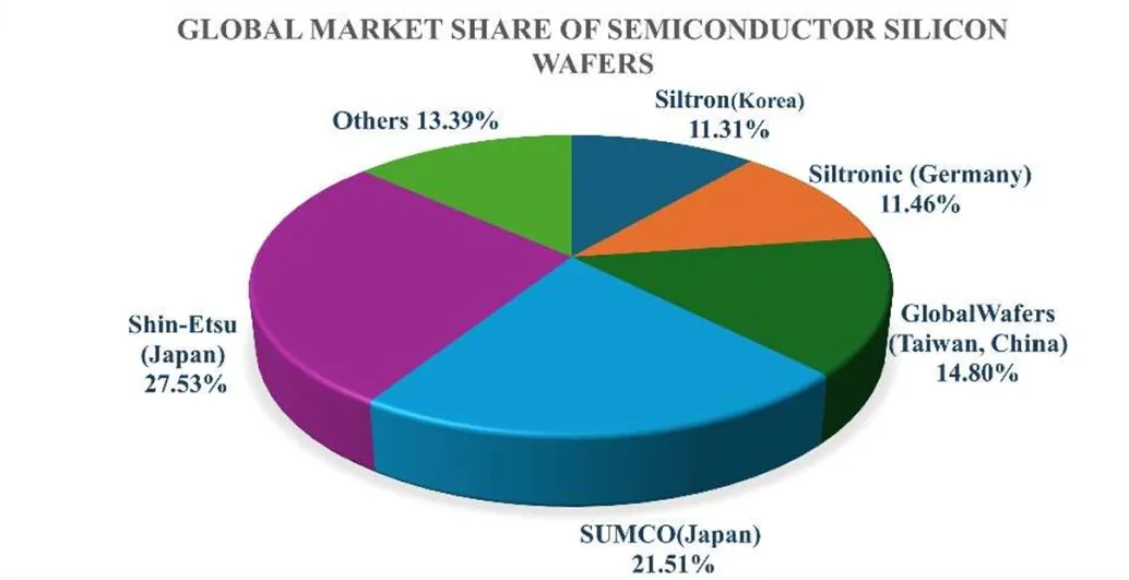
This oligopoly results in China’s heavy dependence on imported monocrystalline silicon wafers, which has become one of the key bottlenecks limiting the development of the country’s integrated circuit industry.
To overcome the current challenges in the semiconductor silicon monocrystal manufacturing sector, investing in research and development and strengthening domestic production capabilities is an inevitable choice.
2. Overview of Monocrystalline Silicon Material
Monocrystalline silicon is the foundation of the integrated circuit industry. To date, over 90% of IC chips and electronic devices are made using monocrystalline silicon as the primary material. The widespread demand for monocrystalline silicon and its diverse industrial applications can be attributed to several factors:
-
Safety and Environmentally Friendly: Silicon is abundant in the Earth’s crust, non-toxic, and environmentally friendly.
-
Electrical Insulation: Silicon naturally exhibits electrical insulation properties, and upon heat treatment, it forms a protective layer of silicon dioxide, which effectively prevents the loss of electrical charge.
-
Mature Growth Technology: The long history of technological development in silicon growth processes has made it far more sophisticated than other semiconductor materials.
These factors together keep monocrystalline silicon at the forefront of the industry, making it irreplaceable by other materials.
In terms of crystal structure, monocrystalline silicon is a material made from silicon atoms arranged in a periodic lattice, forming a continuous structure. It is the basis of the chip manufacturing industry.
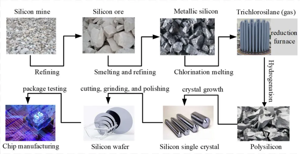
The following diagram illustrates the complete process of monocrystalline silicon preparation:
Process Overview:
Monocrystalline silicon is derived from silicon ore through a series of refining steps. First, polycrystalline silicon is obtained, which is then grown into a monocrystalline silicon ingot in a crystal growth furnace. Afterward, it is cut, polished, and processed into silicon wafers suitable for chip manufacturing.
Silicon wafers are typically divided into two categories: photovoltaic-grade and semiconductor-grade. These two types differ mainly in their structure, purity, and surface quality.
-
Semiconductor-grade wafers have an exceptionally high purity of up to 99.999999999%, and are strictly required to be monocrystalline.
-
Photovoltaic-grade wafers are less pure, with purity levels ranging from 99.99% to 99.9999%, and do not have such stringent requirements for crystal quality.
In addition, semiconductor-grade wafers require higher surface smoothness and cleanliness than photovoltaic-grade wafers. The higher standards for semiconductor wafers increase both the complexity of their preparation and their subsequent value in applications.
The following chart outlines the evolution of semiconductor wafer specifications, which have increased from early 4-inch (100mm) and 6-inch (150mm) wafers to current 8-inch (200mm) and 12-inch (300mm) wafers.
In actual silicon monocrystal preparation, the wafer size varies based on the application type and cost factors. For example, memory chips commonly use 12-inch wafers, while power devices often use 8-inch wafers.
In summary, the evolution of wafer size is the result of both Moore’s Law and economic factors. A larger wafer size enables the growth of more usable silicon area under the same processing conditions, reducing production costs while minimizing waste from wafer edges.
As a crucial material in modern technological development, semiconductor silicon wafers, through precise processes such as photolithography and ion implantation, enable the production of various electronic devices, including high-power rectifiers, transistors, bipolar junction transistors, and switching devices. These devices play a key role in fields such as artificial intelligence, 5G communications, automotive electronics, the Internet of Things, and aerospace, forming the cornerstone of national economic development and technological innovation.
3. Monocrystalline Silicon Growth Technology
The Czochralski (CZ) Method is an efficient process for pulling high-quality monocrystalline material from the melt. Proposed by Jan Czochralski in 1917, this method is also known as the Crystal Pulling method.
Currently, the CZ method is widely used in the preparation of various semiconductor materials. According to incomplete statistics, about 98% of electronic components are made from monocrystalline silicon, with 85% of these components produced using the CZ method.
The CZ method is favored because of its excellent crystal quality, controllable size, rapid growth rate, and high production efficiency. These characteristics make CZ monocrystalline silicon the preferred material for meeting the high-quality, large-scale demand in the electronics industry.
The growth principle of CZ monocrystalline silicon is as follows:
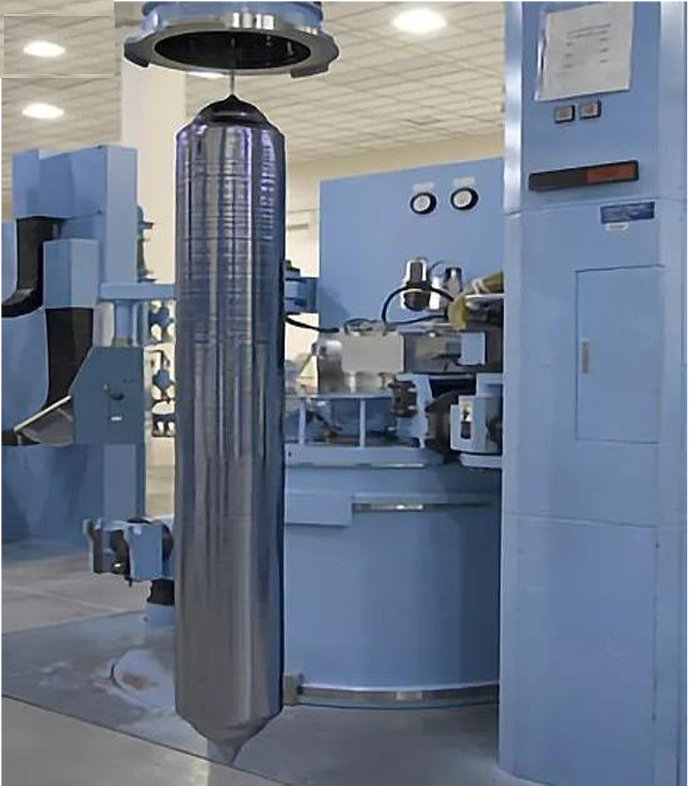
The CZ process requires high temperatures, a vacuum, and a closed environment. The key equipment for this process is the crystal growth furnace, which facilitates these conditions.
The following diagram illustrates the structure of a crystal growth furnace.
In the CZ process, pure silicon is placed in a crucible, melted, and a seed crystal is introduced into the molten silicon. By precisely controlling parameters such as temperature, pull rate, and crucible rotation speed, atoms or molecules at the interface of the seed crystal and molten silicon continuously reorganize, solidifying as the system cools and ultimately forming a single crystal.
This crystal growth technique produces high-quality, large-diameter monocrystalline silicon with specific crystal orientations.
The growth process involves several key steps, including:
-
Disassembly and Loading: Removing the crystal and thoroughly cleaning the furnace and components from contaminants such as quartz, graphite, or other impurities.
-
Vacuum and Melting: The system is evacuated to a vacuum, followed by the introduction of argon gas and the heating of the silicon charge.
-
Crystal Pulling: The seed crystal is lowered into the molten silicon, and the interface temperature is carefully controlled to ensure proper crystallization.
-
Shouldering and Diameter Control: As the crystal grows, its diameter is carefully monitored and adjusted to ensure uniform growth.
-
End of Growth and Furnace Shutdown: Once the desired crystal size is achieved, the furnace is shut down, and the crystal is removed.
The detailed steps in this process ensure the creation of high-quality, defect-free monocrystals suitable for semiconductor manufacturing.
4. Challenges in Monocrystalline Silicon Production
One of the main challenges in producing large-diameter semiconductor monocrystals lies in overcoming the technical bottlenecks during the growth process, particularly in predicting and controlling crystal defects:
-
Inconsistent Monocrystal Quality and Low Yield: As the size of the silicon monocrystals increases, the complexity of the growth environment increases, making it difficult to control factors like the thermal, flow, and magnetic fields. This complicates the task of achieving consistent quality and higher yields.
-
Unstable Control Process: The growth process of semiconductor silicon monocrystals is highly complex, with multiple physical fields interacting, making control precision unstable and leading to low product yields. Current control strategies mainly focus on the macroscopic dimensions of the crystal, while quality is still adjusted based on manual experience, making it difficult to meet the requirements for micro and nano fabrication in IC chips.
To address these challenges, the development of real-time, online monitoring and prediction methods for crystal quality is urgently needed, along with improvements in control systems to ensure stable, high-quality production of large monocrystals for use in integrated circuits.
Post time: Oct-29-2025