At present, our company can continue to supply small batch of 8inchN type SiC wafers, if you have sample needs, please feel free to contact me. We have some sample wafers ready to ship.
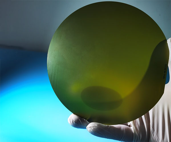
In the field of semiconductor materials, the company has made a major breakthrough in the research and development of large size SiC crystals. By using its own seed crystals after multiple rounds of diameter enlargement, the company has successfully grown 8-inch N-type SiC crystals, which solves difficult problems such as uneven temperature field, crystal cracking and gas phase raw material distribution in the growth process of 8-inch SIC crystals, and accelerates the growth of large size SIC crystals and the autonomous and controllable processing technology. Greatly enhance the company's core competitiveness in the SiC single crystal substrate industry. At the same time, the company actively promotes the accumulation of technology and process of large size silicon carbide substrate preparation experimental line, strengthens the technical exchange and industrial collaboration in upstream and downstream fields, and collaborates with customers to constantly iterate product performance, and jointly promotes the pace of industrial application of silicon carbide materials.
|
8inch N-type SiC DSP Specs |
|||||
| Number | Item | Unit | Production | Research | Dummy |
| 1. Parameters | |||||
| 1.1 | polytype | -- | 4H | 4H | 4H |
| 1.2 | surface orientation | ° | <11-20>4±0.5 | <11-20>4±0.5 | <11-20>4±0.5 |
| 2. Electrical parameter | |||||
| 2.1 | dopant | -- | n-type Nitrogen | n-type Nitrogen | n-type Nitrogen |
| 2.2 | resistivity | ohm ·cm | 0.015~0.025 | 0.01~0.03 | NA |
| 3. Mechanical parameter | |||||
| 3.1 | diameter | mm | 200±0.2 | 200±0.2 | 200±0.2 |
| 3.2 | thickness | μm | 500±25 | 500±25 | 500±25 |
| 3.3 | Notch orientation | ° | [1- 100]±5 | [1- 100]±5 | [1- 100]±5 |
| 3.4 | Notch Depth | mm | 1~1.5 | 1~1.5 | 1~1.5 |
| 3.5 | LTV | μm | ≤5(10mm*10mm) | ≤5(10mm*10mm) | ≤10(10mm*10mm) |
| 3.6 | TTV | μm | ≤10 | ≤10 | ≤15 |
| 3.7 | Bow | μm | -25~25 | -45~45 | -65~65 |
| 3.8 | Warp | μm | ≤30 | ≤50 | ≤70 |
| 3.9 | AFM | nm | Ra≤0.2 | Ra≤0.2 | Ra≤0.2 |
| 4. Stucture | |||||
| 4.1 | micropipe density | ea/cm2 | ≤2 | ≤10 | ≤50 |
| 4.2 | metal content | atoms/cm2 | ≤1E11 | ≤1E11 | NA |
| 4.3 | TSD | ea/cm2 | ≤500 | ≤1000 | NA |
| 4.4 | BPD | ea/cm2 | ≤2000 | ≤5000 | NA |
| 4.5 | TED | ea/cm2 | ≤7000 | ≤10000 | NA |
| 5. Positive quality | |||||
| 5.1 | front | -- | Si | Si | Si |
| 5.2 | surface finish | -- | Si-face CMP | Si-face CMP | Si-face CMP |
| 5.3 | particle | ea/wafer | ≤100(size≥0.3μm) | NA | NA |
| 5.4 | scratch | ea/wafer | ≤5,Total Length≤200mm | NA | NA |
| 5.5 | Edge chips/indents/cracks/stains/contamination |
-- | None | None | NA |
| 5.6 | Polytype areas | -- | None | Area ≤10% | Area ≤30% |
| 5.7 | front marking | -- | None | None | None |
| 6. Back quality | |||||
| 6.1 | back finish | -- | C-face MP | C-face MP | C-face MP |
| 6.2 | scratch | mm | NA | NA | NA |
| 6.3 | Back defects edge chips/indents |
-- | None | None | NA |
| 6.4 | Back roughness | nm | Ra≤5 | Ra≤5 | Ra≤5 |
| 6.5 | Back marking | -- | Notch | Notch | Notch |
| 7. Edge | |||||
| 7.1 | edge | -- | Chamfer | Chamfer | Chamfer |
| 8. Package | |||||
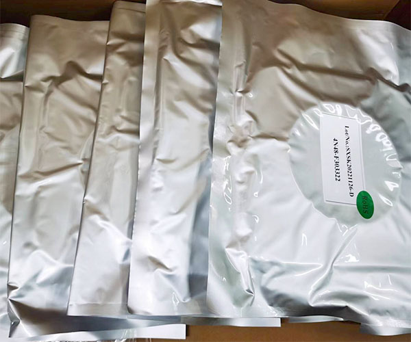
| 8.1 | packaging | -- | Epi-ready with vacuum packaging |
Epi-ready with vacuum packaging |
Epi-ready with vacuum packaging |
| 8.2 | packaging | -- | Multi-wafer cassette packaging |
Multi-wafer cassette packaging |
Multi-wafer cassette packaging |
Post time: Apr-18-2023